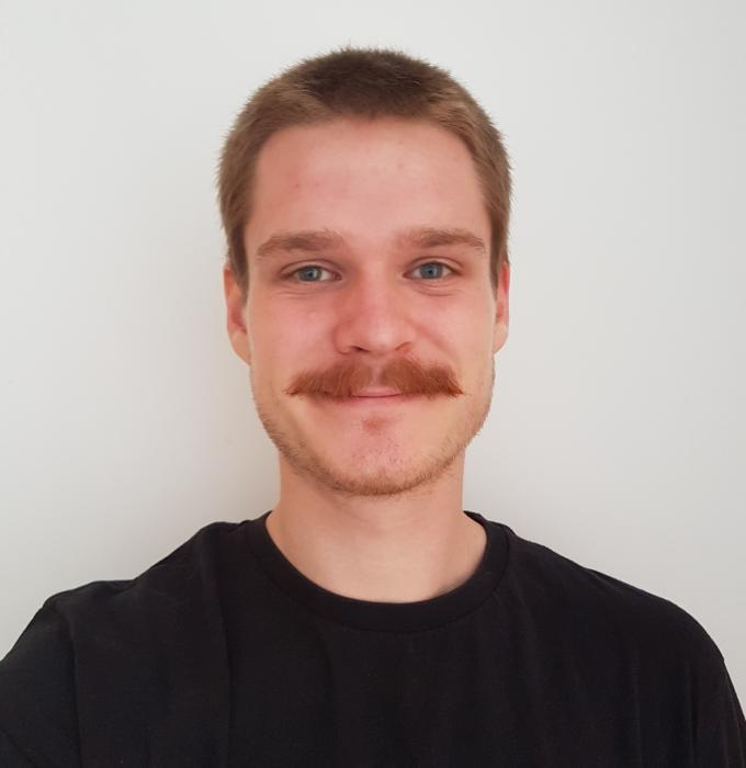
MSc J. Strube
PhD student
Electronic Instrumentation (EI), Department of Microelectronics Themes: Merging (Ultra)-Wide bandgap Sensors with Integrated Circuits
Electronic Instrumentation (EI), Department of Microelectronics Themes: Merging (Ultra)-Wide bandgap Sensors with Integrated Circuits
Biography
I was born in Germany in 1998 and received my B.Eng and M.Sc from the University of Applied Science HTW Berlin. My previous work was concerned with cleanliness of SiC manufacturing techniques for EUV lithography wafer clamps and materials engineering of piezoelectric thin films in bulk acoustic wave RF filters. I joined the TU Delft as PhD researcher in the field of a novel CMOS-integrated 3-dimensional Hall sensor.
Last updated: 15 Feb 2024

Jannik Strube
- [email protected]
- Room: HB 14.030
- Personal webpage
- List of publications